electronics design
fab academy week 6
This week class was about Electronic Design, the class content can be found here.
For this week assignment I am going to make a PCB for my ESP32 Huzzah board for sensors to measure temperature so I can use it to check the performance of the low tech experiments we are making (solar oven and fireless cooker).
We have two types of temperature sensors at the fablab : NTC and RTD. I am going to use a NTC thermistor (Negative Temperature Coefficient Thermistor - they are thermally sensitive resistors and have are decreasing in resistance as temperature increases).
The circuit I want to make should have 2 thermometers and 2 RGB LEDs that will change color depending on the temperature.
- One to measure the temperature inside the solar oven
- The second one to measure the outside temperature
prototype on breadboard
I started to test the termistor wiring on my breadboard with the ESP32 microcontroller. I used a few online tutorials to find out the right wiring. NTC thermistors need to be wired with a resistor to make a voltage divider. NTC resistance decreases as the temperature rises. The Steinhart-Hart equation enables to use this data to derive temperature.I used the following library to calculate and display the temperature on my monitor. Link to the library
I then added some code to change the color of the LED when the temperature is over 20°C. I will use different limits when it will be for the oven but here it was just to try it.
Link to the file with the code
schematic
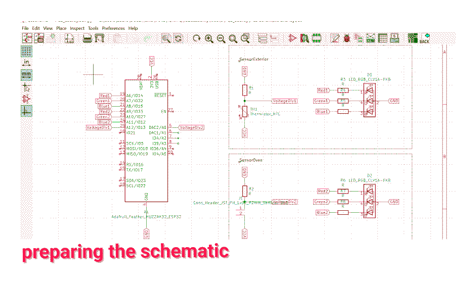
Once the prototype on the breadboard was working, I made the schematic of the wiring on Kicad. We had downloaded before the librairies of components available at FabLab BCN.I duplicated the combination “voltage divider : thermistor + resistor” to have one for the oven and one for the exterior. As the thermistor for the oven would need to be placed inside without putting the whole board in the oven, I changed one of the thermistor for a two pins connector so I will then be able to attach a thermistor to a longer cable that can be placed in the oven.
To make it visually clear, I grouped the connexions into frames (oven sensor, exterior sensor, jumper) and added labels on each wire to represent the connexions between the elements and the micro-controller pins.
The next step is to generate the netlist from the schematic. Then open the netlist in PCB layout editor on Kicad.
Link to my PCB schematic
physical layout
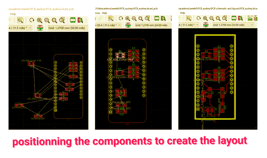
Once I am on the layout editor, the component have connexions that has been automatically generated from the schematic but I need to place them on the board shield to have the most simple circuit possible and avoid circuits to cross. Some people even do “PCB art”, use patterns etc...After moving the components everywhere, I finally found a way to minimize the length of the connexion circuits. I still had two circuits that were crossing so I went back to the schematics and added a resistor that will be 0 ohm to make a jumper as I couldn’t avoid some of the lines to cross. At the end, I created the lines of the outside of the shield and exported it.
Link to my PCB layout
prepare for milling
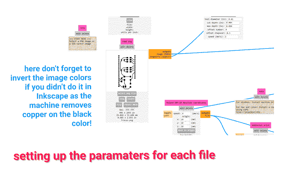
Last step before milling is to prepare the files. I opened the PCB layout from Kicad in Inkscape and separated it into 3 files that have different setup for milling: the holes, the circuit and the outline.It is important to save them with 1000 ppp quality and use custom export to always keep the same size.
When the files were ready, I used MODS to enter the parameters needed for every file, then I saved them to be able to open them with the program of the milling machine.
milling
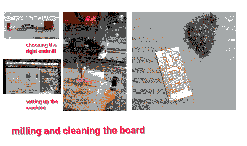
Note: This part is also related to a previous week class “Electronic production”.Here are the steps I followed:
- Tape the PCB with double sided tape
- Open Vpanel for SRM-20
- Place the endmill 1/64 to cut the traces first (be very careful not to make it fall as it is super fragile)
- Place the endmill at the bottom left corner of the board with x and y, then lower the z
- Let endmill “fall” on the board (using the finger to go slow) and screw again
- Set Origin Poin XY and Z
- Press Cut on the program and select the right file
tools I worked with
KicadInkscape
modsproject
Roland SRM-20
learnings
- Don't forget to flip the board shape in Kicad PCB layout editor as it is going to be placed on top of the ESP board
- Make sure lines don't cross when creating the layout
- After cutting clean the board with a metal “brush” and then with alcohol